| |||
TSSDADC2401 - 24-bit Sigma Delta ADC
|
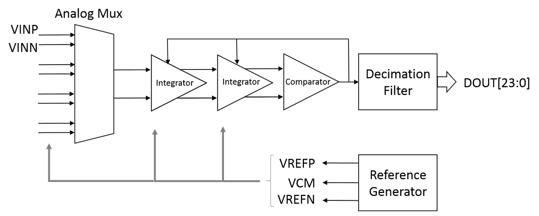
The TSSDADC2401 is a 24-bit analog to digital converter implemented as a Sigma Delta architecture.
The ADC has programmable analog and digital gain settings. Analog gains of 1x or 2x are selected by an analog gain stage before the data converter. Digital gains of 1x, 2x, 4x, 8x, 16x, 32x, 64x and 128x are selected after the digital decimation filter. The ADC supports offset and gain calibration. The calibration routine calibrates the input voltage standard to a digital full-scale output code. The offset and gain calibration results are stored in on-chip registers. The offset and gain calibration results can be overwritten during normal operation. Programmability of the ADC’s decimation filter, digital gain and analog gain allow for tuning of the converter’s data rate, noise and resolution for different modes of operation. The ADC can operate in single-end or differential mode. The digital output formats for single-ended and differential modes are shown in the tables below. |

|
Performance Specifications
|
Parameter |
Description |
Notes/Conditions |
min |
typ |
max |
units |
|
ADCVHIGH |
Input voltage upper limit |
|
|
|
VDD- |
V |
|
ADCVLOW |
Input voltage lower limit |
|
AVSS+ 100mV |
|
|
V |
|
ADCVRANGE |
Input dynamic range |
Single-ended Differential (ADCVHIGH - ADCVLOW) |
0 -VREF |
|
VREF +VREF |
V |
|
|
Common Mode Voltage Range |
|
AVSS+ 100mV |
VDD/2 |
VDD- |
V |
|
ADCRES |
Resolution |
60Hz Notch Mode Resolution @ 10 sps Resolution @ 20 sps Resolution @ 40 sps Resolution @ 80 sps Resolution @ 160 sps Resolution @ 320 sps Resolution @ 640 sps
50Hz Notch Mode Resolution @ 8.333 sps Resolution @ 16.667 sps Resolution @ 33.333 sps Resolution @ 66.667 sps Resolution @ 133.333 sps Resolution @ 266.667 sps Resolution @ 533.333 sps |
|
20.0 19.0 19.0 18.0 16.0 13.0 11.0
20.0 19.0 19.0 18.0 16.0 13.0 11.0 |
|
bits |
|
ADCDNL |
Differential nonlinearity |
|
|
|
±1 |
LSB |
|
ADCINL |
Integral nonlinearity |
Uncalibrated |
|
|
±11 |
LSB |
|
|
Zero Error after calibration |
ppm of full scale reference |
-10 |
|
+10 |
ppm FSR |
|
|
Zero Drift |
zero code drift vs temp |
|
50 |
|
nV/℃ |
|
|
Full Scale Error after calibration |
ppm of full scale reference |
-20 |
|
+20 |
ppm FSR |
|
|
Full Scale Error Drift |
full scale code drift vs temp |
|
0.05 |
|
ppm FSR/℃ |
|
|
Normal Mode 50/60Hz Rejection |
|
100 |
|
|
dB |
|
G |
Input Voltage Gain |
Programmable |
1 |
|
128 |
|
|
|
Data Rate |
Programmable |
2.5 |
10 |
400 |
SPS |
|
VREF |
Reference Voltage |
|
1.8 |
2.5 |
3.2 |
V |
|
VCMO_IN |
Input Common Mode Voltage |
|
100 |
2.5 |
4 |
mV |
|
|
|
|
|
|
|
|
|
|
|
|
|
|
|
|