Proven IC Design Methodology
|
Triad's IC development process uses industry-standard design tools managed by a highly refined design methodology.
Triad's Agile ASIC EDA ToolsFor designs taking advantage of the Agile ASIC flow, Triad uses industry-standard tools augmented with ViaPath™ ViaOnly place and route tools for physical design.
|
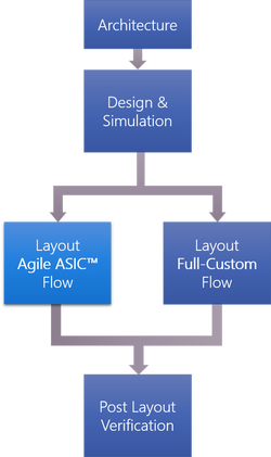
Click image for a detailed view of Triad's IC Design Tool Flow
|
Custom IC EDA Tools
Design &
|
Agile ASIC™
|
Full Custom
|
Post Layout VerificationParasitic Extraction
|
|

|

|

|

|
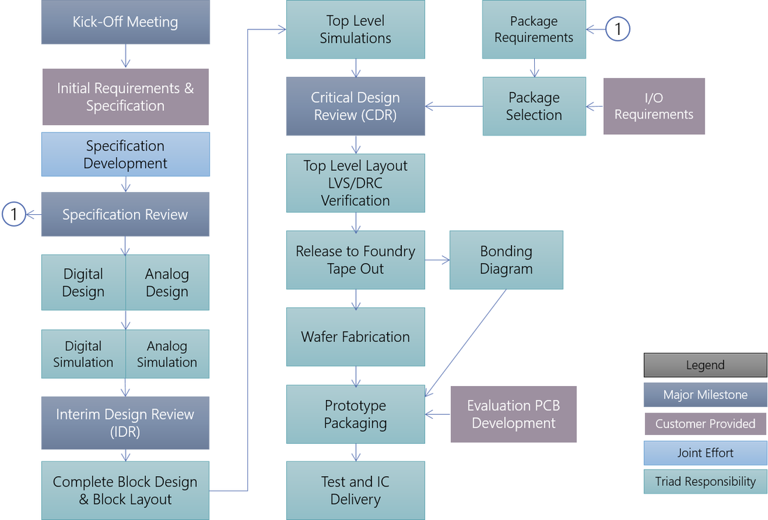
Working With Triad - Typical ASIC Project Flow
High-Level Architecture
Triad's architecture team consisting of an ASIC business expert and mixed-signal IC architect work with your to define a custom IC solution that satisfies your company's technical and business requirements including development cost, development schedule and production unit cost. Project Kickoff Your engineering team meets the Triad team at 1-2 day meeting hosted at our headquarters in Winston-Salem. We walk you through how to successfully execute an ASIC program. You have face-to-face time to immediately start making progress on a detailed implementation specification for your ASIC. |
Click for larger image
| ||
Working Together
Your custom IC will be developed by a dedicated Triad IC design team consisting of a Project Leader, IC Design Team Members and a Project Coordinator. We will hold weekly video conference calls to review project status, track issues, manage tasks. The Project Coordinator will provide you with a weekly report showing how your project is progressing and identifying tasks to be completed by both companies. You have an open line of communication with your Triad IC design team. You can email and call your team as needed during the week to make real-time progress on discussion points without waiting for the weekly status meeting.
It is our expectation that much of the project will be managed via daily email, phone calls and the weekly status call. We have also found that having a few key meetings face-to-face make for the most successful projects.
Recommended Face-to-Face Meetings
Specification Development
You provide your Triad engineering team with your initial requirements and specification that you have developed thus far. At this point in the project, some customers come with a highly refined and detailed set of requirements. On the other hand, some customers have little more than a block diagram or schematic of their discrete circuit. Either way, Triad's engineering team excels a converting your ideas and requirements into an Implementation Specification that will drive the development of your ASIC. Towards the end of the Specification Development phase of the project, we will jointly hold a Specification Review to agree on a the spec for your custom IC.
Design and Simulation
Triad's IC design team translates your requirements contained in the Implementation Specification into detailed analog and digital circuits. Circuits are verified against the implementation specification with extensive analog, digital and mixed-signall simulation.
Interim Design Review (IDR)
After the specification is signed off at the specification review, the design team will begin to develop all of the IP blocks necessary to build the ASIC. Weekly WebEx meetings with the customer will continue during this phase, with email exchanges and one-on-one phone calls, as needed.
When most of the IP blocks have been captured in schematics or in RTL code, Triad will hold an interim design review (IDR) with the customer. The purpose of the IDR is to present completed schematics and simulation results of most, if not all, of the IP blocks on the ASIC.
The IDR is typically an all-day WebEx meeting where Triad engineers present the following:
Complete Block Design & Block Layout
Finalize the design of all low-level blocks in the design. Any required specification refines identified in the IDR meeting are implemented at this point. Agile ASIC block-level design includes the design of low-level transistor circuits along with full-integrated routing fabric. Agile ASIC block design is governed by Triad's Three Laws of ASIC Agility.
Triad's Three Laws of ASIC Agility
Top Level Simulations
Analog, digital and mixed-signal simulations are performed on the top-level design. Triad has developed a flexible simulation methodology that allows for selective control of implementation detail for top-level simulations. Different blocks can be represented as high-level models such as Verilog-A or VHDL-AMS while other blocks are detailed transistor-level SPICE models. This approach allows for extensive test coverage and accelerated simulation.
Critical Design Review (CDR)
Following the IDR, the design team will continue development of the IP blocks necessary to build the ASIC.
This activity will include:
During this phase, weekly WebEx meetings with the customer will continue, with email exchanges and one-on-one phone calls, as needed. The CDR is typically held about 4 weeks before Triad expects to tape out the ASIC.
The CDR itself is an all-day face-to-face meeting where Triad engineers typically present the following:
Top Level Layout and Release for Fabrication
The verified low-level blocks are assembled in the final custom IC. Note, in an Agile ASIC flow blocks or reconfigurable tiles can be assembled long before the circuit is finished because circuit changes can be implemented on the tiles by making ViaOnly changes. In Triad's Hyper Agile ASIC flow, the base layers of the design can actually be released to the foundry before the circuit has been completed. This approach can offer significant savings over traditional full-custom-only approaches.
The next major milestone is release to fabrication, also called "tape out". Triad engineering will only release the ASIC for fabrication if a list of exit criteria have been satisfied. Some of the checks included are:
Prototype Delivery
Once fabrication of the wafers is completed, the wafer fab will ship the wafers to one of Triad’s package assembly suppliers. The assembly house will package enough die from the wafers to provide Triad and the customer with prototype units for use in lab evaluation, production test development, and reliability testing.
The assembly house will then ship the packaged ASICs to Triad. Triad will typically screen an agreed upon number of packaged ASICs with a manual test routine and ship acceptable ASICs to the customer. The acceptance criteria will usually only include basic functionality at this point.
Prototype Evaluation
Both Triad and the customer will evaluate the performance of the ASIC with customer-provided PC boards. Since both parties are using the same board layout, correlation of lab results is achieved with less difficulty.
Triad will verify that the ASIC meets specification by testing and characterizing several ASICs over power supply and temperature. The results of these tests will be placed into a compliance matrix which will will highlight any failures of the ASIC to be spec compliant. The compliance matrix will be shared with the customer and compared to the customer’s evaluation results.
All specifications that the ASIC fails to meet will be flagged and there will be an agreement between Triad and the customer about how to address the non-compliance.
Also during this phase, production test development will be underway with Triad’s test supplier. The production test plan is written by Triad engineering and given to the supplier to implement on their automated test equipment (ATE). The production test plan will provide test coverage sufficient to verify functionality of the ASIC, including any critical specifications that can be tested with the ATE. As ATE is limited in capability in order to deliver high-speed testing, any specifications not tested by ATE will have to be verified by the previously mentioned characterization compliance matrix.
During this phase, quality engineering will initiate reliability testing of the ASIC. This testing will be defined in a reliability plan that has been agreed to by Triad and the customer. Reliability testing includes, at a minimum, ESD and latchup testing.
Design re-work (as necessary)
If the ASIC is non-compliant to the ASIC specification, and both Triad and the customer agree that an ASIC re-design is needed, Triad will initiate re-design of the portions of the ASIC which are not spec compliant. Typically, when the ASIC has been designed as a new via-configurable array (VCA), Triad will be able to only change a single via layer in the layout to successfully re-design the ASIC.
Re-spin Critical Design Review (CDR2)
When the re-design has been completed and Triad is within a couple of weeks of tapeout of the second die revision, Triad will host another CDR. This CDR will typically include the following:
Release to Fabrication
Once the second revision of the ASIC is ready for release to fabrication, or tapeout, Triad engineering will again perform the following checks:
Second Silicon Delivery
Once fabrication of the wafers is completed, the wafer fab will ship the wafers to one of Triad’s package assembly suppliers. The assembly house will package enough die from the wafers to provide Triad and the customer with prototype units for use in lab evaluation, production test development, and reliability testing.
The assembly house will then ship the packaged ASIC’s to Triad. Triad will typically screen an agreed upon number of packaged ASICs with a manual test routine and ship acceptable ASICs to the customer.
Second Silicon Evaluation
Both Triad and the customer will evaluate the performance of the ASIC with customer-provided PC boards. Since both parties are using the same board layout, correlation of lab results is achieved with less difficulty.
Triad will verify that the ASIC meets specification by testing and characterizing several ASICs over power supply and temperature. The results of these tests will be placed into a compliance matrix which will will highlight any failures of the ASIC to be spec compliant. The compliance matrix will be shared with the customer and compared to the customer’s evaluation results.
Special emphasis will be placed on validating that the design changes made for the Si re-spin were successful. Based on Triad’s track record, most of the time the single via-layer re-spin is sufficient to address all design problems found in the first prototypes.
Assuming that the ASIC meets specification, production test development will be completed during this phase. Once the production test software and hardware has been signed off by Triad, all future deliveries of the ASIC will go through the production test flow.
Also during this phase, quality engineering will complete all reliability testing of the ASIC. These results will be shared with the customer.
Production Release
Production release is an internal milestone for Triad which signals that the ASIC is ready to be shipped to the customer and that the following documents have been released:
We require that the final IC specification be signed by the customer before releasing to production. After production release, the ASIC is turned over completely to the Operations team.
Your custom IC will be developed by a dedicated Triad IC design team consisting of a Project Leader, IC Design Team Members and a Project Coordinator. We will hold weekly video conference calls to review project status, track issues, manage tasks. The Project Coordinator will provide you with a weekly report showing how your project is progressing and identifying tasks to be completed by both companies. You have an open line of communication with your Triad IC design team. You can email and call your team as needed during the week to make real-time progress on discussion points without waiting for the weekly status meeting.
It is our expectation that much of the project will be managed via daily email, phone calls and the weekly status call. We have also found that having a few key meetings face-to-face make for the most successful projects.
Recommended Face-to-Face Meetings
- Project Kickoff - held at Triad's HQ in Winston-Salem, NC
- Interim Design Review
- Critical Design Review
Specification Development
You provide your Triad engineering team with your initial requirements and specification that you have developed thus far. At this point in the project, some customers come with a highly refined and detailed set of requirements. On the other hand, some customers have little more than a block diagram or schematic of their discrete circuit. Either way, Triad's engineering team excels a converting your ideas and requirements into an Implementation Specification that will drive the development of your ASIC. Towards the end of the Specification Development phase of the project, we will jointly hold a Specification Review to agree on a the spec for your custom IC.
Design and Simulation
Triad's IC design team translates your requirements contained in the Implementation Specification into detailed analog and digital circuits. Circuits are verified against the implementation specification with extensive analog, digital and mixed-signall simulation.
Interim Design Review (IDR)
After the specification is signed off at the specification review, the design team will begin to develop all of the IP blocks necessary to build the ASIC. Weekly WebEx meetings with the customer will continue during this phase, with email exchanges and one-on-one phone calls, as needed.
When most of the IP blocks have been captured in schematics or in RTL code, Triad will hold an interim design review (IDR) with the customer. The purpose of the IDR is to present completed schematics and simulation results of most, if not all, of the IP blocks on the ASIC.
The IDR is typically an all-day WebEx meeting where Triad engineers present the following:
- any updates to the specification
- schematics of completed analog IP blocks
- simulation results of completed analog IP blocks
- RTL code of completed digital IP blocks
- simulation results of completed digital IP blocks
- schedule review
- supply chain review
Complete Block Design & Block Layout
Finalize the design of all low-level blocks in the design. Any required specification refines identified in the IDR meeting are implemented at this point. Agile ASIC block-level design includes the design of low-level transistor circuits along with full-integrated routing fabric. Agile ASIC block design is governed by Triad's Three Laws of ASIC Agility.
Triad's Three Laws of ASIC Agility
- The circuit shall achieve the performance specification.
- Circuits are made reconfigurable to ensure attaining the desired performance through ViaOnly™ changes.
- Maintain the die size budget when adding reconfigurability.
Top Level Simulations
Analog, digital and mixed-signal simulations are performed on the top-level design. Triad has developed a flexible simulation methodology that allows for selective control of implementation detail for top-level simulations. Different blocks can be represented as high-level models such as Verilog-A or VHDL-AMS while other blocks are detailed transistor-level SPICE models. This approach allows for extensive test coverage and accelerated simulation.
Critical Design Review (CDR)
Following the IDR, the design team will continue development of the IP blocks necessary to build the ASIC.
This activity will include:
- Refinement of analog block schematics
- Simulation of analog blocks over process, voltage, and temperature
- Refinement of RTL coding of digital blocks
- Simulation of digital blocks over process, voltage, and temperature
- Simulations of the full ASIC
- Physical layout of IP blocks
- Physical layout of the top level of the ASIC
During this phase, weekly WebEx meetings with the customer will continue, with email exchanges and one-on-one phone calls, as needed. The CDR is typically held about 4 weeks before Triad expects to tape out the ASIC.
The CDR itself is an all-day face-to-face meeting where Triad engineers typically present the following:
- any updates to the specification
- spec compliance based on simulation results
- updated schematics of analog IP blocks, along with simulation results over process, voltage, and temperature
- updated RTL code of digital IP blocks, along with simulation results over process, voltage, and temperature
- ASIC top level layout
- schedule review
- supply chain review
- next steps to get to tapeout
- action items update
Top Level Layout and Release for Fabrication
The verified low-level blocks are assembled in the final custom IC. Note, in an Agile ASIC flow blocks or reconfigurable tiles can be assembled long before the circuit is finished because circuit changes can be implemented on the tiles by making ViaOnly changes. In Triad's Hyper Agile ASIC flow, the base layers of the design can actually be released to the foundry before the circuit has been completed. This approach can offer significant savings over traditional full-custom-only approaches.
The next major milestone is release to fabrication, also called "tape out". Triad engineering will only release the ASIC for fabrication if a list of exit criteria have been satisfied. Some of the checks included are:
- Simulation, static timing analysis, and formal verification of digital IP
- Top level simulations run with final top level netlist
- Top level layout verification completed (LVS, DRC)
- Bonding diagram verified against ASIC specification and layout of ASIC
- Current revision of ASIC specification signed off by customer
Prototype Delivery
Once fabrication of the wafers is completed, the wafer fab will ship the wafers to one of Triad’s package assembly suppliers. The assembly house will package enough die from the wafers to provide Triad and the customer with prototype units for use in lab evaluation, production test development, and reliability testing.
The assembly house will then ship the packaged ASICs to Triad. Triad will typically screen an agreed upon number of packaged ASICs with a manual test routine and ship acceptable ASICs to the customer. The acceptance criteria will usually only include basic functionality at this point.
Prototype Evaluation
Both Triad and the customer will evaluate the performance of the ASIC with customer-provided PC boards. Since both parties are using the same board layout, correlation of lab results is achieved with less difficulty.
Triad will verify that the ASIC meets specification by testing and characterizing several ASICs over power supply and temperature. The results of these tests will be placed into a compliance matrix which will will highlight any failures of the ASIC to be spec compliant. The compliance matrix will be shared with the customer and compared to the customer’s evaluation results.
All specifications that the ASIC fails to meet will be flagged and there will be an agreement between Triad and the customer about how to address the non-compliance.
Also during this phase, production test development will be underway with Triad’s test supplier. The production test plan is written by Triad engineering and given to the supplier to implement on their automated test equipment (ATE). The production test plan will provide test coverage sufficient to verify functionality of the ASIC, including any critical specifications that can be tested with the ATE. As ATE is limited in capability in order to deliver high-speed testing, any specifications not tested by ATE will have to be verified by the previously mentioned characterization compliance matrix.
During this phase, quality engineering will initiate reliability testing of the ASIC. This testing will be defined in a reliability plan that has been agreed to by Triad and the customer. Reliability testing includes, at a minimum, ESD and latchup testing.
Design re-work (as necessary)
If the ASIC is non-compliant to the ASIC specification, and both Triad and the customer agree that an ASIC re-design is needed, Triad will initiate re-design of the portions of the ASIC which are not spec compliant. Typically, when the ASIC has been designed as a new via-configurable array (VCA), Triad will be able to only change a single via layer in the layout to successfully re-design the ASIC.
Re-spin Critical Design Review (CDR2)
When the re-design has been completed and Triad is within a couple of weeks of tapeout of the second die revision, Triad will host another CDR. This CDR will typically include the following:
- any updates to the specification
- spec compliance based on simulation results
- updated schematics of analog IP blocks, along with simulation results over process, voltage, and temperature
- updated RTL code of digital IP blocks, along with simulation results over process, voltage, and temperature
- schedule review
- supply chain review
- next steps to get to tapeout
- action items update
Release to Fabrication
Once the second revision of the ASIC is ready for release to fabrication, or tapeout, Triad engineering will again perform the following checks:
- Simulation, static timing analysis, and formal verification of digital IP (if changed)
- Top level simulations with final top level netlist
- Top level layout verification completed (LVS, DRC)
- Bonding diagram verified against ASIC specification and layout of ASIC
- Current revision of ASIC specification signed off by customer
Second Silicon Delivery
Once fabrication of the wafers is completed, the wafer fab will ship the wafers to one of Triad’s package assembly suppliers. The assembly house will package enough die from the wafers to provide Triad and the customer with prototype units for use in lab evaluation, production test development, and reliability testing.
The assembly house will then ship the packaged ASIC’s to Triad. Triad will typically screen an agreed upon number of packaged ASICs with a manual test routine and ship acceptable ASICs to the customer.
Second Silicon Evaluation
Both Triad and the customer will evaluate the performance of the ASIC with customer-provided PC boards. Since both parties are using the same board layout, correlation of lab results is achieved with less difficulty.
Triad will verify that the ASIC meets specification by testing and characterizing several ASICs over power supply and temperature. The results of these tests will be placed into a compliance matrix which will will highlight any failures of the ASIC to be spec compliant. The compliance matrix will be shared with the customer and compared to the customer’s evaluation results.
Special emphasis will be placed on validating that the design changes made for the Si re-spin were successful. Based on Triad’s track record, most of the time the single via-layer re-spin is sufficient to address all design problems found in the first prototypes.
Assuming that the ASIC meets specification, production test development will be completed during this phase. Once the production test software and hardware has been signed off by Triad, all future deliveries of the ASIC will go through the production test flow.
Also during this phase, quality engineering will complete all reliability testing of the ASIC. These results will be shared with the customer.
Production Release
Production release is an internal milestone for Triad which signals that the ASIC is ready to be shipped to the customer and that the following documents have been released:
- IC Specification
- IC Layout (GDS)
- Bonding Diagram
- Branding Diagram
- Reliability Test Plan
- Manufacturing Plan
- Production Test Plan
- Customer Notification Letter
- Production Documentation Checklist
- Tape and Reel Requirements
- Assembly Build Sheet
We require that the final IC specification be signed by the customer before releasing to production. After production release, the ASIC is turned over completely to the Operations team.
