Family of Projective Capacitive Touch Sensor Agile ASICs™
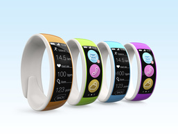
Touchscreen technology is everywhere. Many technologies have been used for touchscreen applications including resistive, acoustic and capacitive. The projected capacitive touchscreen approach has proven to be both high-performance and cost-effective for many applications. In touch applications, high-performance means delivering high-resolution touch recognition coupled with high scan rates to support multi-touch and palm discrimination algorithms.
Capacitive Touchscreen Implementation Challenges

Capacitive touch solutions rely on an orthogonal grid of "virtually invisible" traces that are overlaid on top of the display surface. When a finger comes close to the screen, capacitance changes occur, and these changes are registered by many the 'nodes' where these traces intersect. Software algorithms translate these capacitance values into an X, Y-coordinate indicating where the user is touching the screen. As displays get larger, the number of rows and columns in a cap-touch matrix grow. Assume that horizontal traces drive the cap-touch matrix and that the vertical traces sense touches. Ideally, the cap-touch drivers would be located near the drive traces and the receivers would likewise be located near the receiver traces. As the display gets larger, it is difficult to minimize trace length with a single device that combines drivers and receivers in the same IC.
|
As screens get larger, the following must be considered:
|

|
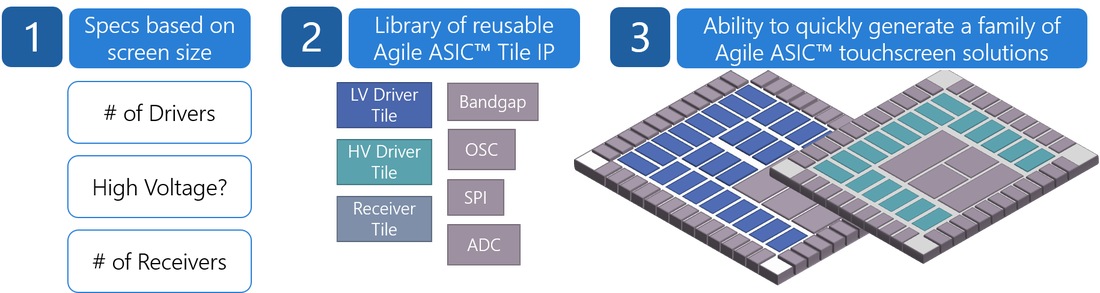
Capacitive Touch Sensor ASIC Solutions Need to Be Optimized by Screen Size
After considering the requirements, the customer determined that three different solutions were required to support the different screen sizes associated with different markets.
- Small screens such as tablets could use a unified driver/receiver ASIC as the low-cost solution.
- Larger screens needed a chipset consisting of a driver ASIC and receiver ASIC to accommodate the mechanical and electrical requirements of keeping drivers near the driver traces and receivers near the sense traces.
- Even larger screens needed the ability to use multiple driver and receiver chips with the added performance boost delivered by using higher drive voltages.
Why The Customer Chose Triad's Agile ASIC™ Solution
The customer worked with Triad to specify a highly reusable set of cap-touch driver and receiver circuits. These circuits were carefully optimized for performance and die area and realized as Agile ASIC™ Tile IP. |
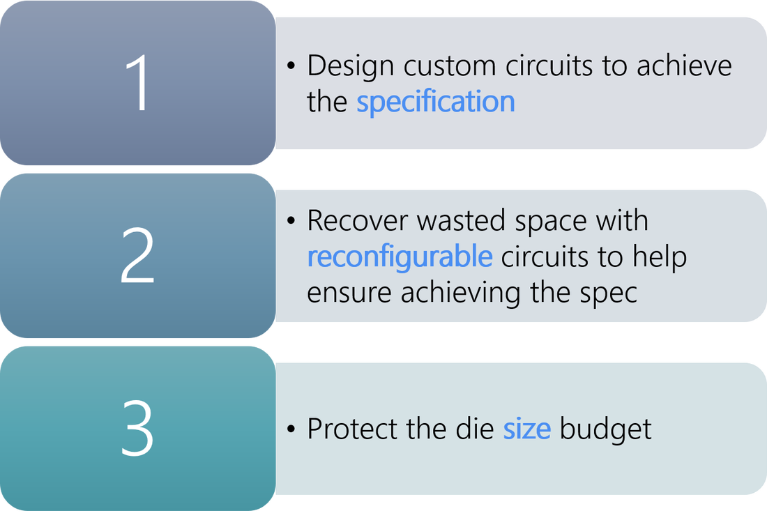
Triad's Three Laws of Agility
|
An Agile Approach to Developing a Family of Capacitive Touch Sensor ASICs
Triad's Agile ASIC solutions are ViaOnly™ reconfigurable. This means that analog, digital, and mixed-signal design changes can be made in the ASIC quickly and cost-effectively. Additionally, Triad's Agile ASIC Tile IP represents the industry's fastest and most effective IP reuse strategy. Agile ASIC Tiles contain both circuits and highly-optimized routing fabric. These tiles "snap-together" when placed in a layout grid. The use of Agile ASIC Tile IP allowed the customer to quickly generate a family of capacitive touch Agile ASIC solutions that were both performance and cost optimized.
The Design Worked to Spec, Yet Failed in the System - Agile Change Management
After embarking on this project, a common mixed-signal ASIC development problem occurred. The first prototypes were fabricated and the design worked to the specification but failed in the system. The load capacitance for the touchscreen drivers had been underspecified by a factor of twenty. This was a major problem and the defect was replicated some forty times, once for each output driver.

In a typical full-custom design, this type of problem would have been catastrophic. There was no hope of a simple metal-only change to fix the problem. An entirely new circuit was needed.
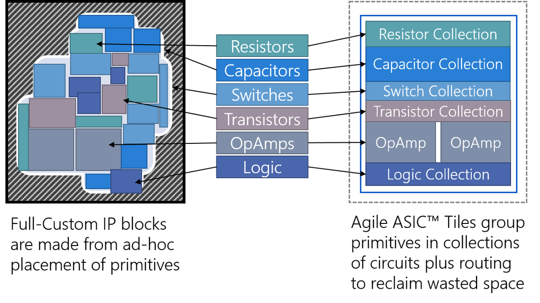
All custom ICs contain spare resources. In a full-custom design, sub-blocks end up as amorphous shapes due to the local optimizing of silicon area. During top-level assembly, these amorphous shapes become more wasteful because they get enclosed in floorplanning black boxes. Full-custom designers attempt to place spare resources haphazardly in the unused gaps left in the top-level layout. Unfortunately, it is statistically unlikely that this ad-hoc placement of resources will be able to realize a design fix that satisfies sensitive analog performance requirements.
Effective and predictable analog change management relies on having the right resources in proximity to the circuit needing repair. And, these resources need access to metal routing to effect repairs. Effective mixed-signal change management places fine-grain repair resources and routing fabric in proximity to the circuits under repair.
Triad's Agile ASIC Tiles Deliver an Effective and Predictable Analog Change Management StrategyAn Agile ASIC tile is a systematic arrangement of analog circuit primitives and routing fabric into resource collections. These collections contain 'unit' capacitor and resistors, transistor fingers, switches, logic elements, and configurable operational amplifier circuits. Resistor or capacitors of a given value are built out of these collections by placing vias in the routing fabric to interconnect unit resources.
|
|
Transistors of varying W/L ratios are similarly built by configuring "transistor fingers" into larger composite resources. The amorphously shaped full custom circuit is enclosed in a rectangular black-box. The area outside of the full custom circuit but inside the black-box is wasted space in a traditional full-custom design. In an Agile ASIC, the wasted area of the black box is reclaimed. For example, spare resistors are placed in the resistor collection along with routing resources to reclaim area that would be wasted in a full-custom design. This process is repeated in the other collection areas (capacitors, switches, e.tc). These spare resources are tied off until needed and do not consume power. Often, unused resources will be converted into decoupling capacitors that help to filter local power delivery to the tile. These spare resources do not increase the area of the IP block.
A given Agile Tile may or may not be larger than a single full-custom implementation. The overall efficiency of interconnecting an entire chip of Agile Tiles often means that even in very high production volumes, an Agile ASIC will have the same overall die size budget as an equivalent full-custom design.
A given Agile Tile may or may not be larger than a single full-custom implementation. The overall efficiency of interconnecting an entire chip of Agile Tiles often means that even in very high production volumes, an Agile ASIC will have the same overall die size budget as an equivalent full-custom design.
Agile ASIC Change Management for the Capacitive Touch Sensor ASIC
|
The customer had a major circuit problem (the output drive was off by a factor of twenty), and the problem was replicated in each driver. Fortunately, each of these driver circuits was implemented as Agile ASIC Tile IP. The circuit topology needed significant changes that would have been impossible in a full-custom only layout.
The Triad engineer on the project quoted that it would take a week to make the design changes and verify the circuit. In actuality, he solved the problem over a long weekend. In the Agile ASIC approach, the new circuit was created at the schematic level and simulated. The rest of the design process was fully automated. Triad schematic elements either map directly to Agile ASIC Tile primitives or composite components are synthesized from Triad's ViaWare™ software. The resultant netlist was processed by Triad's ViaPath™ mixed-signal aware ViaOnly place and route software. Circuits were placed in the Agile ASIC and routed by the placement of vias. Vias were used to configure and interconnect resources within the device. ViaPath's advanced constraint system allowed circuits that are verified to go through the incremental routing process untouched to preserve well-performing functions while repairing and refining other circuit areas. The process from net listing through place and route and final design rule checking (DRC) was completed in hours. A problem that could have taken months to fix by hand was fixed in hours and days with Triad's Agile ASIC approach. New chips were fabricated, packaged and shipped to the customer. The new version of the design was certified as production worthy allowing the customer to meet their aggressive production schedule. |
Triad's Agile ASIC Approach fixed in a long weekend what would have been an impossible problem in a traditional full-custom-only design. 
|
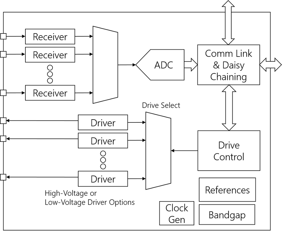
Agile ASIC™ Solution Touchscreen Driver Receiver
|


Agile ASIC™ Solution -
Projected Capacitive Touchscreen Receiver
|
Circuit Details
- Family of projected capacitive touchscreen controllers
- Ability to rapidly and cost effectively create touchscreen controllers optimized for a given screen size
- Combined drivers and receivers in a single ASIC for smaller displays
- A two chip solution of a low-voltage driver IC and a receiver IC for larger displays
- A daisy-chain-able high-voltage driver IC and low-voltage receiver IC for the largest display sizes
- Precision analog front end (AFE)
- Data converters
- Serial communications like with daisy-chaining
IP Blocks Utilized
- Cap-touch low voltage driver tile
- Cap-touch high voltage driver tile
- Cap-touch low voltage receiver tile
- Band Pass Filter
- Analog to Digital Conversion
- Combined Analog and Digital Automatic Gain Control (AGC)
- Bandgap, Precision Reference Network
- SPI, custom daisy-chaining link
Learn more about
Triad's Consumer Electronics ASICs
Triad's Consumer Electronics ASICs
|